

What is inside a PCB factory in China?
Please don’t underestimate the process of turning the designed schematic diagram into a real PCB circuit board. There are many things that are feasible in principle but difficult to realize in engineering.
Or what other people can achieve, others cannot. Therefore, it is not difficult to make a PCB board, but it is not an easy task to make a good PCB board.
The videos we publish will help you understand the PCB making process, Wonderful PCB provides one-stop PCB assembly service.
Clear design goals
When a design task is received, its design goals must first be clarified.
PCB, high-frequency PCB, small-signal processing PCB or PCB with both high-frequency and small-signal processing. For long lines, it is necessary to use certain means to deal with them, reduce the load, and strengthen the drive for long lines, and the key point is to prevent long line reflections.
When there are signal lines exceeding 40MHz on the board, special consideration must be given to these signal lines, such as crosstalk between lines. If the frequency is higher, there are stricter restrictions on the length of wiring. According to the network theory of distributed parameters, the interaction between high-speed circuits and their connections is a decisive factor, which cannot be ignored in system design.
As the gate transmission speed increases, the opposition on the signal line will increase accordingly, and the crosstalk between adjacent signal lines will increase proportionally. Usually, the power consumption and heat dissipation of high-speed circuits are also very large. When making high-speed PCB should be given sufficient attention.
When there are weak signals of millivolt level or even microvolt level on the board, special attention should be paid to these signal lines. Because the small signal is too weak, it is very easy to be interfered by other strong signals. Shielding measures are often necessary, otherwise it will be damaged. Significantly reduces the signal-to-noise ratio. As a result, useful signals are submerged by noise and cannot be extracted effectively.
The commissioning of the board should also be considered in the design stage. Factors such as the physical location of the test point and the isolation of the test point cannot be ignored, because some small signals and high-frequency signals cannot be directly added to the probe for measurement.
In addition, other related factors should be considered, such as the number of layers, the package shape of components, and the mechanical strength of the board.
Understand the layout and routing requirements of the functions of the components used
We know that some special components have special requirements when layout and wiring, such as the analog signal amplifier used by APH, the analog signal amplifier requires stable power supply and small ripple. The analog small signal part should be kept away from power devices as far as possible.
Component Layout Considerations
One of the first factors to be considered in the layout of components is electrical performance. Put components with close connections together as much as possible, especially for some high-speed lines, make it as short as possible when laying out, power signals and small signal devices to separate.
On the premise of satisfying the circuit performance, it is also necessary to consider that the components are placed neatly, beautifully, and easy to test. The mechanical size of the board and the position of the socket also need to be carefully considered.
Wiring Considerations
With the completion of the design of OTNI and star optical fiber network, there will be more boards with high-speed signal lines above 100MHz to be designed. Here we will introduce some basic concepts of high-speed lines.
Transmission line
For integrated circuits, due to the increase in edge speed, if no other measures are taken, the length of the trace must be greatly shortened to maintain the integrity of the signal.
At higher bit rates and faster edge rates when there is fan-out along the signal line, the TTL shaping method described above is somewhat insufficient. Because there are reflected waves in the line, they will tend to be synthesized at high bit rates, causing severe signal distortion and reduced anti-interference ability.
Therefore, in order to solve the reflection problem, another method is usually used in the ECL system: the line impedance matching method. In this way, the reflection can be controlled and the integrity of the signal can be guaranteed.
Strictly speaking, transmission lines are not very necessary for conventional TTL and CMOS devices with slower edge speeds.
Transmission lines are also not always necessary for high-speed ECL devices with faster edge speeds. But when used with transmission lines, they have the advantage of being able to predict line delays and control reflections and oscillations through impedance matching.
Several types of transmission lines
Coaxial cable and twisted pair: These are often used for system-to-system connections. The characteristic impedance of the coaxial cable is usually 50Ω and 75Ω, and the twisted pair is usually 110Ω.
Microstrip lines on printed boards
A microstrip line is a strip conductor (signal line). Separated from the ground plane by a dielectric. If the line’s thickness, width, and distance from the ground plane are controllable, its characteristic impedance is also controllable. :
Stripline in printed boards
A stripline is a copper strip line placed in the middle of a dielectric between two conductive planes. If the thickness and width of the line, the dielectric constant of the medium, and the distance between the two conductive planes are controllable, then the characteristic impedance of the line is also controllable, and the characteristic impedance of the strip line is:
Terminated Transmission Line
When the receiving end of a line is terminated with a resistor equal to the characteristic impedance of the line, the transmission line is called a parallel terminal connection. It is mainly used to obtain the best electrical performance, including driving distributed loads.
Sometimes in order to save power consumption, a 104 capacitor is connected in series with the terminating resistor to form an AC terminating circuit, which can effectively reduce DC loss.
A resistor is connected in series between the driver and the transmission line, and the end of the line is no longer connected to the termination resistor. This termination method is called series termination.
Overshoot and ringing on longer lines can be controlled with series damping or series termination techniques. Series damping is achieved by using a small resistor (typically 10-75Ω) in series with the output of the drive gate.
This damping method is suitable for use with lines whose characteristic impedance is controlled (such as backplane wiring, circuit boards without a ground plane, and most wound wires, etc.).
The sum of the value of the series resistance and the output impedance of the circuit (driver gate) when terminated in series is equal to the characteristic impedance of the transmission line. The series-connected terminal wiring has the disadvantages that only lumped loads can be used at the terminal and the transmission delay time is relatively long. However, this can be overcome by using redundant series-terminated transmission lines.
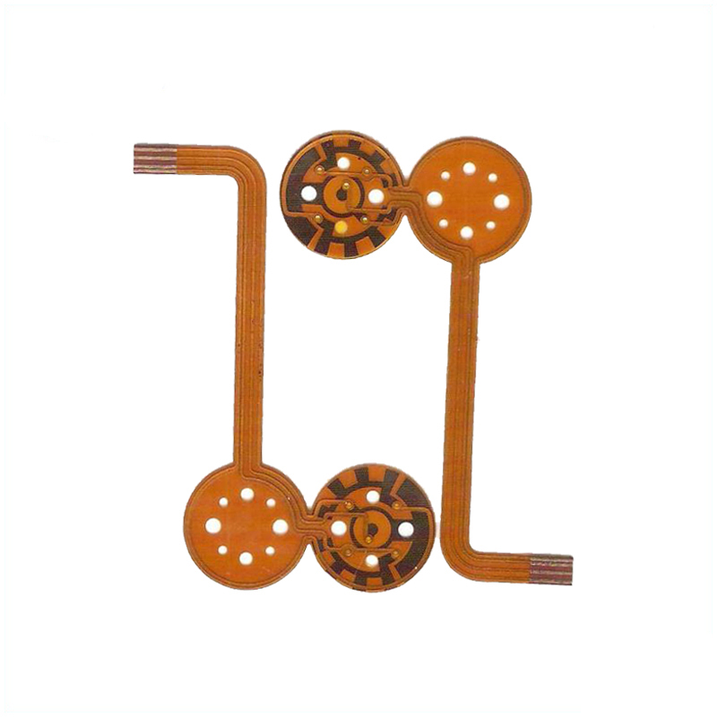
(Picture of Wonderful PCB)
unterminated transmission line
Transmission lines can be used without series or parallel termination if the line delay time is much shorter than the signal rise time, and if the round-trip delay (the time it takes a signal to make one round trip on the transmission line) of an unterminated line is shorter than that of a pulse If the rise time of the signal is short, the kickback due to non-termination is about 15% of the logic swing.
The maximum open line length is approximately:
Both parallel terminal wiring and series terminal wiring have their own advantages. Which one or both are used depends on the designer’s hobbies and system requirements.
The main advantages of parallel terminal wiring are fast system speed and signal transmission on the line without distortion.
Loading on a long line will neither affect the propagation delay time of the drive gate driving the long line nor its signal edge speed, but will increase the propagation delay time of the signal along the long line.
When driving a large fan-out, the load can be distributed along the line through the branch stub, instead of having to collect the load at the terminal of the line as in the series termination.
The series termination method enables the circuit to have the ability to drive several parallel load lines. The delay time increment caused by the capacitive load of the series terminal wiring is about twice that of the corresponding parallel terminal wiring, and the short line is caused by the capacitive load. The speed is slowed down and the drive gate delay time is increased.
However, the crosstalk of the series terminal wiring is smaller than that of the parallel terminal wiring. The main reason is that the signal amplitude transmitted along the series terminal wiring is only one-half of the logic swing, so the switch current is only the switching current of the parallel terminal connection. Half, the signal energy is small and the crosstalk is small.
Whether to choose a double-sided board or a multi-layer board when making a PCB depends on the highest operating frequency, the complexity of the circuit system, and the requirements for assembly density. When the clock frequency exceeds 200MHZ, it is best to choose a multi-layer board.
If the working frequency exceeds 350MHz, it is best to use a printed circuit board with polytetrafluoroethylene as the dielectric layer, because its high-frequency attenuation is smaller, the parasitic capacitance is smaller, and the transmission speed is faster. Large and power-saving, the following principle requirements are required for the wiring of printed circuit boards:
All parallel signal lines should be spaced as far apart as possible to reduce crosstalk. If there are two signal lines that are close to each other, it is best to run a ground wire between the two lines, which can play a shielding role.
When designing the signal transmission line, sharp turns should be avoided to prevent reflections caused by sudden changes in the characteristic impedance of the transmission line, and it should be designed as a uniform arc line with a certain size as much as possible.
The width of the printed line can be calculated according to the above-mentioned characteristic impedance calculation formula of the microstrip line and stripline. The characteristic impedance of the microstrip line on the printed circuit board is generally between 50-120Ω.
In order to obtain a large characteristic impedance, the line width must be made very narrow. Considering various factors, it is generally more appropriate to choose an impedance value of about 68Ω, because choosing a characteristic impedance of 68Ω can achieve the best balance between delay time and power consumption.
A 50Ω transmission line will consume more power; although a larger impedance can reduce power consumption, it will increase the transmission delay time. Due to the negative line capacitance, the transmission delay time will increase and the characteristic impedance will decrease.
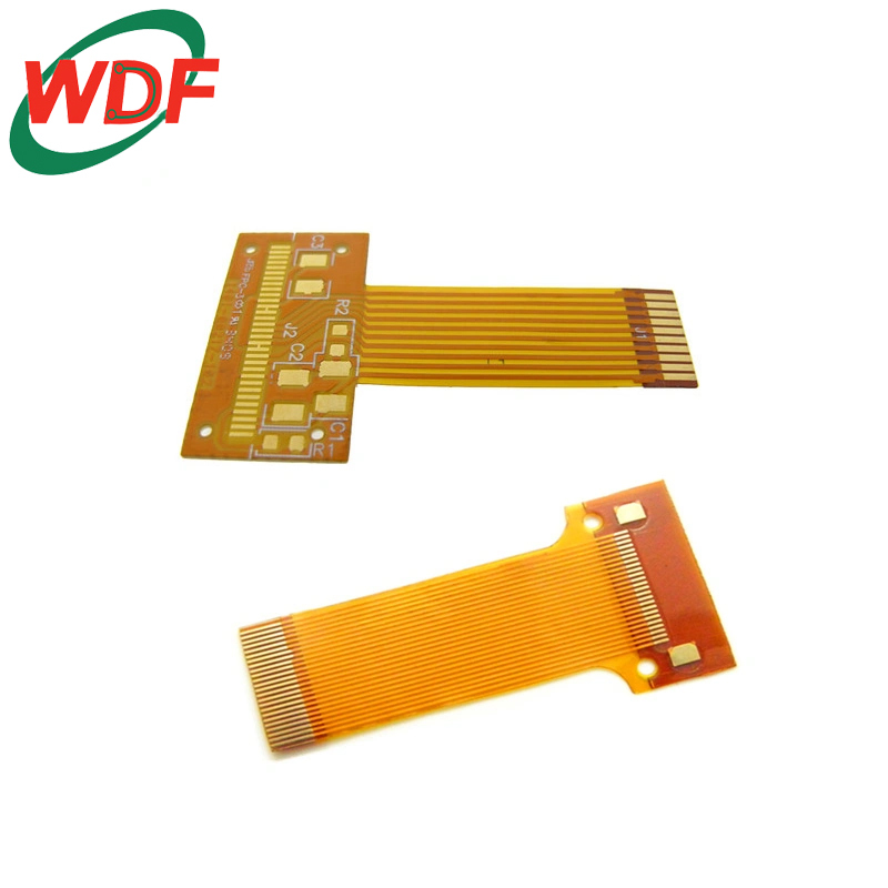
(Picture of Wonderful PCB)
However, the intrinsic capacitance per unit length of the line segment with very low characteristic impedance is relatively large, so the transmission delay time and characteristic impedance are less affected by the load capacitance. An important characteristic of a properly terminated transmission line is that stubs should have little effect on line delay time.
When Z0 is 50Ω. The length of short branches must be limited within 2.5cm.
The lines on both sides of the circuit board should be perpendicular to each other to prevent crosstalk caused by mutual induction.
If there are high-current devices on the printed board, such as relays, indicator lights, speakers, etc., it is best to separate their ground wires to reduce noise on the ground wire.
The ground wires of these high-current devices should be connected to an independent ground bus on the plug-in board and the backplane, and these independent ground wires should also be connected to the ground point of the entire system.
If there is a small signal amplifier on the board, the weak signal line before amplification should be far away from the strong signal line, and the wiring should be as short as possible, and if possible, it should be shielded with a ground wire.
About Wonderful


Shenzhen Wonderful Technology Co., Ltd. is China’s top model and small batch circuit board manufacturer.
The company targets precision circuit board samples and small batches as the main target market. Since its establishment, it has adhered to the development concept of good quality and important reputation.
Invest huge sums of money to introduce advanced equipment, strictly regulate the operating standards and QC standards for incoming and outgoing materials, to ensure that the shipped products reach Seiko quality.
The self-developed ERP management system can realize the whole process of paperless operations such as online ordering, online payment, online production progress query, online logistics tracking, and online statistical report production, which greatly improves work efficiency.
It ensures that each order can be shipped quickly. After more than ten years of development, the company’s products and services have been well received by the market.
As well as the opening of an electronic component mall, integrated circuits, semiconductors, resistors, capacitors and other products are sold.
The company’s scale is developing rapidly, and the sample and small batch shipment capacity reaches 500 models/day.
The products are widely used in communications, medical equipment, industrial control products, aviation, military products, testing instruments,Automotive, computers and other peripheral products.
We will continue to pay attention to customers, with efficient delivery speed and perfect after-sales service, to become the most trusted brand supplier in the PCB industry.
Wonderful PCB You can send us your requirements first. Click here to contact us.
You can click our component store. Please click here to contact us.


 English